- 您现在的位置:买卖IC网 > Sheet目录308 > ADUM5402WCRWZ (Analog Devices Inc)IC ISOLATOR 4CH DCDC CONV 16SOIC
�� �
�
�ADuM5401W/ADuM5402W/ADuM5403W�
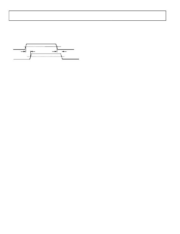
�PROPAGATION� DELAY� RELATED� PARAMETERS�
�Propagation� delay� is� a� parameter� that� describes� the� time� it� takes�
�a� logic� signal� to� propagate� through� a� component� (see� Figure� 24).�
�The� propagation� delay� to� a� logic� low� output� may� differ� from� the�
�propagation� delay� to� a� logic� high.�
�Data� Sheet�
�As� a� result,� the� ADuM5401W/ADuM5402W/ADuM5403W�
�devices� can� draw� large� amounts� of� current� at� low� voltage� for�
�extended� periods� of� time.�
�The� output� voltage� of� the� ADuM5401W/ADuM5402W/�
�ADuM5403W� devices� exhibits� VISO� overshoot� during� startup.�
�INPUT� (V� Ix� )�
�OUTPUT� (V� Ox� )�
�t� PLH�
�t� PHL�
�50%�
�50%�
�If� this� overshoot� could� potentially� damage� components� attached�
�to� V� ISO� ,� a� voltage-limiting� device� such� as� a� Zener� diode� can� be�
�used� to� clamp� the� voltage.� Typical� behavior� is� shown� in� Figure� 17�
�and� Figure� 18.�
�Figure� 24.� Propagation� Delay� Parameters�
�Pulse� width� distortion� is� the� maximum� difference� between� these�
�two� propagation� delay� values� and� is� an� indication� of� how�
�accurately� the� input� signal� timing� is� preserved.�
�Channel-to-channel� matching� refers� to� the� maximum� amount�
�the� propagation� delay� differs� between� channels� within� a� single�
�ADuM5401W/ADuM5402W/ADuM5403W� component.�
�Propagation� delay� skew� refers� to� the� maximum� amount� the�
�propagation� delay� differs� between� multiple� ADuM5401W/�
�ADuM5402W/ADuM5403W� components� operating� under�
�the� same� conditions.�
�START-UP� BEHAVIOR�
�The� ADuM5401W/ADuM5402W/ADuM5403W� do� not�
�contain� a� soft� start� circuit.� Therefore,� the� start-up� current� and�
�voltage� behavior� must� be� taken� into� account� when� designing�
�with� these� devices.�
�When� power� is� applied� to� V� DD1� ,� the� input� switching� circuit� begins�
�to� operate� and� draw� current� when� the� UVLO� minimum� voltage�
�is� reached.� The� switching� circuit� drives� the� maximum� available�
�power� to� the� output� until� it� reaches� the� regulation� voltage� where�
�PWM� control� begins.� The� amount� of� current� and� the� time�
�required� to� reach� regulation� voltage� depends� on� the� load� and�
�the� V� DD1� slew� rate.�
�With� a� fast� V� DD1� slew� rate� (200� μs� or� less),� the� peak� current� draws�
�up� to� 100� mA/V� of� V� DD1� .� The� input� voltage� goes� high� faster� than�
�the� output� can� turn� on;� therefore,� the� peak� current� is� propor-�
�tional� to� the� maximum� input� voltage.�
�With� a� slow� V� DD1� slew� rate� (in� the� millisecond� range),� the� input�
�voltage� is� not� changing� quickly� when� V� DD1� reaches� the� UVLO�
�minimum� voltage.� The� current� surge� is� approximately� 300� mA�
�because� V� DD1� is� nearly� constant� at� the� 2.7� V� UVLO� voltage.� The�
�behavior� during� startup� is� similar� to� when� the� device� load� is� a�
�short� circuit;� these� values� are� consistent� with� the� short-circuit�
�current� shown� in� Figure� 12.�
�When� starting� the� device� for� V� ISO� =� 5� V� operation,� do� not� limit�
�the� current� available� to� the� V� DD1� power� pin� to� less� than� 300� mA.�
�The� ADuM5401W/ADuM5402W/ADuM5403W� devices� may�
�not� be� able� to� drive� the� output� to� the� regulation� point� if� a�
�current-limiting� device� clamps� the� V� DD1� voltage� during� startup.�
�EMI� CONSIDERATIONS�
�The� dc-to-dc� converter� section� of� the� ADuM5401W/ADuM5402W/�
�ADuM5403W� components� must,� of� necessity,� operate� at� a� very�
�high� frequency� to� allow� efficient� power� transfer� through� the� small�
�transformers.� This� creates� high� frequency� currents� that� can�
�propagate� in� circuit� board� ground� and� power� planes,� causing�
�edge� and� dipole� radiation.� Grounded� enclosures� are� recom-�
�mended� for� applications� that� use� these� devices.� If� grounded�
�enclosures� are� not� possible,� follow� good� RF� design� practices� in�
�the� layout� of� the� PCB.� See� the� AN-0971� Application� Note� for�
�board� layout� recommendations.�
�DC� CORRECTNESS� AND� MAGNETIC� FIELD�
�IMMUNITY�
�Positive� and� negative� logic� transitions� at� the� isolator� input� cause�
�narrow� (~1� ns)� pulses� to� be� sent� to� the� decoder� via� the� transformer.�
�The� decoder� is� bistable� and� is,� therefore,� either� set� or� reset� by�
�the� pulses,� indicating� input� logic� transitions.� In� the� absence� of�
�logic� transitions� at� the� input� for� more� than� 1� μs,� periodic� sets� of�
�refresh� pulses� indicative� of� the� correct� input� state� are� sent� to�
�ensure� dc� correctness� at� the� output.� If� the� decoder� receives� no�
�internal� pulses� for� more� than� approximately� 5� μs,� the� input� side�
�is� assumed� to� be� unpowered� or� nonfunctional,� in� which� case,�
�the� isolator� output� is� forced� to� a� default� low� state� by� the� watchdog�
�timer� circuit.� This� situation� should� occur� only� during� power-up�
�and� power-down� operations.�
�The� limitation� on� the� magnetic� field� immunity� of� the�
�ADuM5401W/ADuM5402W/ADuM5403W� is� set� by� the�
�condition� in� which� induced� voltage� in� the� receiving� coil� of� the�
�transformer� is� sufficiently� large� to� either� falsely� set� or� reset� the�
�decoder.� The� following� analysis� defines� the� conditions� under�
�which� this� can� occur.�
�The� pulses� at� the� transformer� output� have� an� amplitude� of� >1.0� V.�
�The� decoder� has� a� sensing� threshold� of� about� 0.5� V,� thus� estab-�
�lishing� a� 0.5� V� margin� in� which� induced� voltages� can� be� tolerated.�
�The� voltage� induced� across� the� receiving� coil� is� given� by�
�V� =� (� ?dβ/dt� )∑π� r� n2� ;� n� =� 1,� 2,� …� ,� N�
�where:�
�β� is� the� magnetic� flux� density� (gauss).�
�r� n� is� the� radius� of� the� n� th� turn� in� the� receiving� coil� (cm).�
�N� is� the� number� of� turns� in� the� receiving� coil.�
�Given� the� geometry� of� the� receiving� coil� in� the� ADuM5401W/�
�ADuM5402W/ADuM5403W,� and� an� imposed� requirement� that�
�Rev.� D� |� Page� 20� of� 24�
�发布紧急采购,3分钟左右您将得到回复。
相关PDF资料
ADUM5404CRWZ
IC ISOLATOR 4CH DCDC CONV 16SOIC
ADUM6132ARWZ-RL
IC GATE DRIVER ISOLATED 16-SOIC
ADUM6201CRIZ
ISOLATED DC-DC CONV 2CH 16SOIC
ADUM6404ARWZ
IC ISOLATOR 4CH DCDC CONV 16SOIC
ADUM7241CRZ-RL7
ISOLATOR DGTL 1KVRMS 2CH 8SOIC
ADUM7440CRQZ-RL7
IC DIGITAL ISOLATOR 4CH 16QSOP
ADUM7510BRQZ
IC DGTL ISOLATOR 5CH 16QSOP
ADZS-21364-EZLITE
KIT EVAL EZ LITE ADDS-21364
相关代理商/技术参数
ADUM5402WCRWZ-1
功能描述:ISOLATOR 4CH DCDC CONV 16SOIC RoHS:是 类别:隔离器 >> 数字隔离器 系列:* 产品培训模块:IsoLoop® Isolator 标准包装:50 系列:IsoLoop® 输入 - 1 侧/2 侧:5/0 通道数:5 电源电压:3 V ~ 5.5 V 电压 - 隔离:2500Vrms 数据速率:110Mbps 传输延迟:12ns 输出类型:CMOS 封装/外壳:16-SOIC(0.154",3.90mm 宽) 供应商设备封装:16-SOIC N 包装:管件 工作温度:-40°C ~ 85°C 其它名称:390-1053-5
ADUM5402WCRWZ-1RL
功能描述:ISOLATOR 4CH DCDC CONV 16SOIC RoHS:是 类别:隔离器 >> 数字隔离器 系列:* 产品培训模块:IsoLoop® Isolator 标准包装:50 系列:IsoLoop® 输入 - 1 侧/2 侧:5/0 通道数:5 电源电压:3 V ~ 5.5 V 电压 - 隔离:2500Vrms 数据速率:110Mbps 传输延迟:12ns 输出类型:CMOS 封装/外壳:16-SOIC(0.154",3.90mm 宽) 供应商设备封装:16-SOIC N 包装:管件 工作温度:-40°C ~ 85°C 其它名称:390-1053-5
ADUM5402WCRWZ-RL
功能描述:IC ISOLATOR 4CH DCDC CONV 16SOIC RoHS:是 类别:隔离器 >> 数字隔离器 系列:IsoPower®, iCoupler® 产品培训模块:IsoLoop® Isolator 标准包装:50 系列:IsoLoop® 输入 - 1 侧/2 侧:5/0 通道数:5 电源电压:3 V ~ 5.5 V 电压 - 隔离:2500Vrms 数据速率:110Mbps 传输延迟:12ns 输出类型:CMOS 封装/外壳:16-SOIC(0.154",3.90mm 宽) 供应商设备封装:16-SOIC N 包装:管件 工作温度:-40°C ~ 85°C 其它名称:390-1053-5
ADUM5402WXRWZ
功能描述:DGTL ISO 2.5KV GEN PURP 16SOIC 制造商:analog devices inc. 系列:* 零件状态:上次购买时间 标准包装:1
ADUM5403
制造商:AD 制造商全称:Analog Devices 功能描述:Quad-Channel, 2.5 kV Isolators with Integrated DC-to-DC Converter
ADUM5403ARWZ
功能描述:IC ISOLATOR 4CH DCDC CONV 16SOIC RoHS:是 类别:隔离器 >> 数字隔离器 系列:IsoPower®, iCoupler® 标准包装:66 系列:iCoupler® 输入 - 1 侧/2 侧:2/2 通道数:4 电源电压:3.3V,5V 电压 - 隔离:2500Vrms 数据速率:25Mbps 传输延迟:60ns 输出类型:逻辑 封装/外壳:20-SSOP(0.209",5.30mm 宽) 供应商设备封装:20-SSOP 包装:管件 工作温度:-40°C ~ 105°C
ADUM5403ARWZ1
制造商:AD 制造商全称:Analog Devices 功能描述:Quad-Channel Isolators with Integrated DC-to-DC Converter
ADUM5403ARWZ2
制造商:AD 制造商全称:Analog Devices 功能描述:Quad-Channel Isolators with Integrated DC-to-DC Converter